wikiHow is a “wiki,” similar to Wikipedia, which means that many of our articles are co-written by multiple authors. To create this article, 44 people, some anonymous, worked to edit and improve it over time.
This article has been viewed 395,768 times.
Learn more...
So you have that circuit designed and ready. You did some computer aided simulations and the circuit is working great. Only one thing left! You need to create a printed circuit board so you can see it in action! Whether your circuit is a project for school/college or is a final piece of electronics in a professional product for your company, implementing your circuit on a PCB will give it a much more professional appearance and give you an idea of how the finished product will look!
Steps
Printing the Circuit Board
-
1Choose a method to use for creating the PCB. Your choice will usually be based on the availability of materials needed by the method, the technical difficulty level of the method or the quality of PCB you desire to obtain. Here's a brief summary of the different methods and their main features that will help you decide:
- Acid etching method: this method requires extreme safety measure, the availability of many materials such as the etchant and it is somewhat slow. The quality of PCB obtained varies according to the materials you use but generally, it is a good method for simple to intermediate levels of complexity circuits. Circuits involving more close wiring and tiny wires usually use other methods.
- UV etching method: this method is used for transposition of your PCB layout onto your PCB board and requires more expensive materials that might not be available everywhere. However, the steps are relatively simple and can produce finer and more complicated circuit layouts.
- Mechanical etching/routing method: this method requires special machines that will mechanically etch away unnecessary copper from the board or route empty separators between wires. It can be expensive if you intend to buy one of those machines and usually leasing them requires the availability of a workshop nearby. However, this method is good if you need to create many copies of the circuit and also can produce fine PCBs.
- Laser etching method: this is usually used by large production companies, but can be found on some universities. The concept is similar to mechanical etching but LASER beams are used to etch the board. It is usually hard to access such machines, but if your local university is one of the lucky ones having such machine, you can use their facilities if they allow it.
-
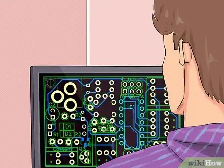
2Create the PCB Layout of your circuit. For acid etching, you need to draw the circuitry using an etchant resistant material. Special markers can be found easily for this specific purpose if you intend to do the drawing by hand (not appropriate for medium to large circuits). Laser printers' ink is the most commonly used material however. This is usually done by converting your circuit's schematic diagram into a PCB layout using PCB layout software. There are many open source software packages for PCB layout creation and design, some are listed here to give you a head-start:Advertisement
-
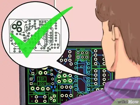
3Once you are happy with the schematic on your computer, match the size of the diagram on the software so that both the circuit board and the paper will have the needed sizes.
-
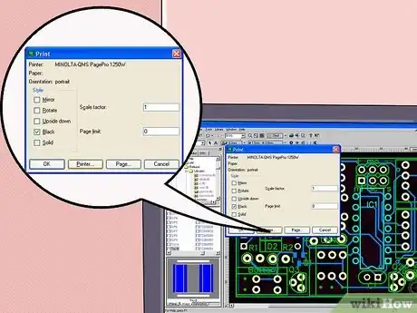
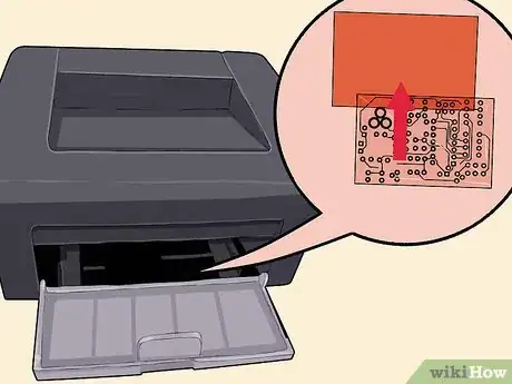
4Print out the diagram from the software's File menu. Print it out on a glossy paper, such as magazine paper. You should ensure the circuit is mirrored before doing that (most PCB layout programs have this as an option when printing). Once printed, make sure you don’t touch the ink part on the paper as it can get on your hands.
-
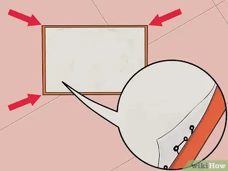
5Align the circuit diagram on the paper with the circuit board (the diagram should be facing the copper part of the circuit board). Start up your iron. Set the iron on the cotton setting and wait until it heats up.
-
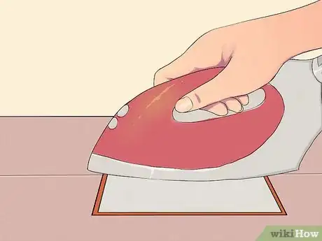
6Once heated, carefully place the iron on top of the paper which is on top of the circuit board.
-
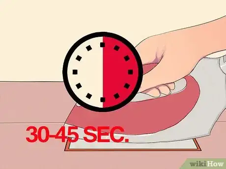
7Place the iron there for about 30-45 seconds (depending on your iron).
-
8After lifting the iron, put it aside carefully and take the circuit board to your nearest source of water. Be careful, the paper will be hot. The paper should be stuck to the circuit board, don’t rip it out.
-
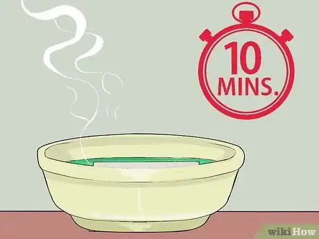
9Start the water flow and hold the circuit board below it. An alternative approach is to immerse the board and paper in hot water for a few minutes (up to 10 minutes).
-
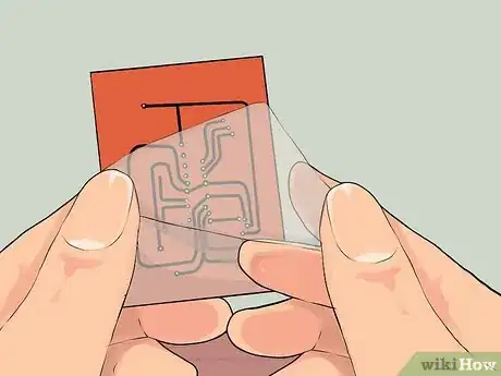
10Slowing start taking off the paper and soon all of the paper should come off. If certain areas seem particularly difficult to peel off, you can try soaking a bit more. If everything went well, you will have a copper board with your PCB pads and signal lines traced out in black toner.
-
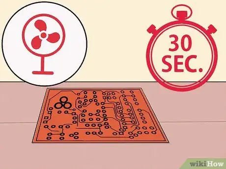
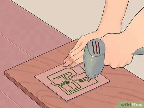
11Dry the board. Get the big droplets of water off by softly wiping with a napkin or sponge or just letting them fall out. It shouldn’t take more than 30 seconds and it should not be vigorous or else the ink on to the circuit might come off.
-
12Etch the board using one of the methods below. This process removes any unnecessary copper from the board leaving only wiring of the final circuit.
Etching with Acid
-
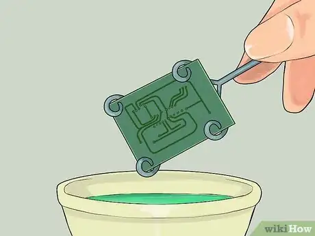
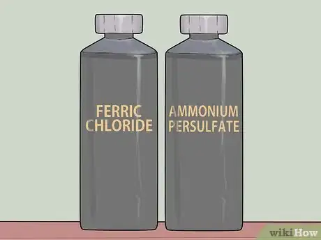
1Choose your etching acid. Ferric chloride is a common choice for an etchant. However, you can use Ammonium Persulfate crystals or other chemical solutions. No matter what choice for the chemical etchant, it will always be a dangerous material, so besides following the general safety precautions mentioned in this article, you should also read and follow any additional safety instructions that come with the etchant.
-
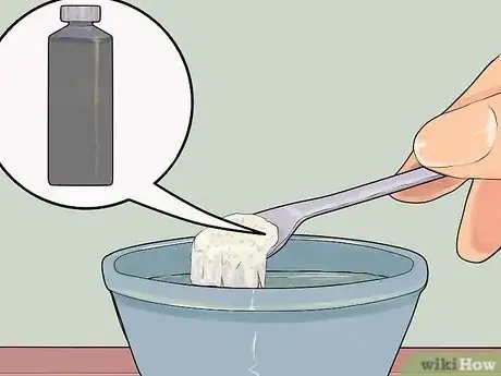
2Prepare the acid etchant. Depending on the acid etch that you choose, there might be additional instructions. For example, some crystallized acids require being dissolved in hot water, but other etchants are ready to use.
-
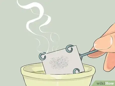
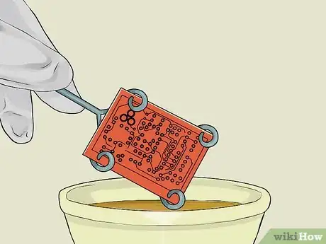
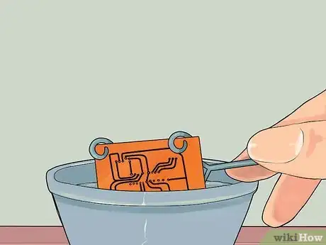
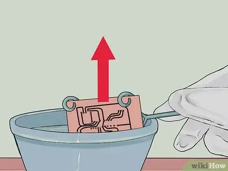
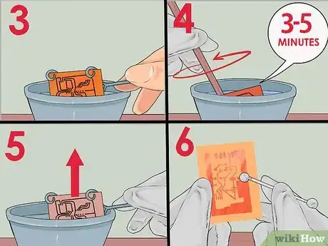
3Submerge the board in the acid.
-
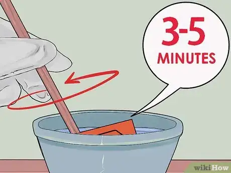
4Make sure to stir every 3-5 minutes.
-
5Take the board out and wash it when all unnecessary copper is etched away from the board.
-
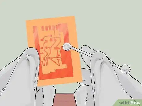
6Remove the insulating drawing material used. There are special solvents available for almost all types of insulating drawing material used in drawing PCB layouts. However, if you don't have access to any of these materials, you can always use a sandpaper (a fine one).
Etching with Ultra-Violet Transposition
-
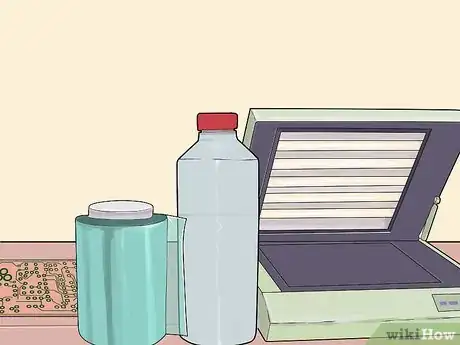
1To apply with this method, you will need a photosensitive (positive or negative) laminated PCB card, an UV insulator and a transparent sheet and distilled water. You may find the cards ready to use (they are covered with a black nylon sheet), or photosensitive spray to apply on the copper side of an ordinary blank PCB card. Take care to purchase also a photorevelator compatible with the photo spray or the PCB photosensitive coating.
-
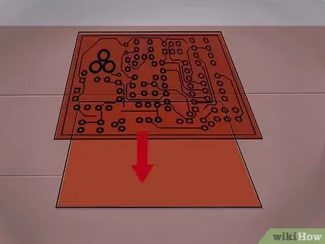
2With a laser printer, draw the PCB layout on the transparent sheet, in positive or negative mode, according to the photosensitive coating of the card.
-
3Cover the copper side of the board with the printed transparent sheet.
-
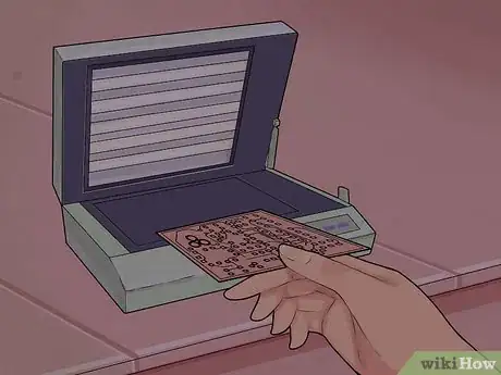
4Place the board in the UV insulator machine/chamber.
-
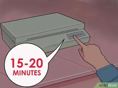
5Turn on the UV machine. It will irradiate your board with the UV for the specified amount of time. Most of the UV insulators are equipped with an adjustable timer. Generally, 15 to 20 minutes will be widely sufficient.
-
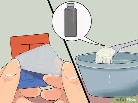
6Once done, remove the board from the UV insulator. Clean the copper side of the card with the photorevelator, then gently rinse the revelated PCB card with distilled water prior to place it in its acid bath. The parts destroyed by the UV irradiation will be etched by the acid.
-
7The further steps to follow are described in the acid etching method specific steps 3 to 7.
Finishing the Board
Community Q&A
-
QuestionWhat is the technical difference between a charger, a power supply, and a battery?
 ShadowspawnfoxxyCommunity AnswerA charger will charge a portable battery or power supply. A power supply allows direct non-changeable power to a computer or system. A battery is a container that carries its own portable power supply.
 -
QuestionDoes the printing of the circuit on the CU board require any special ink?
 Priyanshu MishraCommunity AnswerNo. The toner of the laser printer is sufficient. Only use a laser printer.
 -
QuestionIs there any software that will actively allow me to create a circuit on a virtual PCB?
 RetroAsgardianCommunity AnswerFritzing is a good software package for creating circuits and laying them out on PCBs.
Warnings
- If you are using the acid etching method, you need to take the following precautions:
- Always store your acid in a safe cold place. Use glass containers.
- Label your acid and store it somewhere out of the reach of children and pets.
- Do not dispose of your used acid in the home drains. Instead store it and when you have some amount of used acid, take it to your recycling center/dangerous waste disposal facility.
- Use gloves and air masks when working with acid etchants.
- Be extremely careful when mixing and stirring the acid. Do not use metallic objects and do not put the container on the edge of the disk.
- While irradiating your PCB with UV, take an absolute care to not have a direct visual contact with the UV generating part of the insulator/chamber, or use special anti-UV protection glasses. If you have to check your PCB during the process, better stop the machine prior to open it.
⧼thumbs_response⧽ - Make sure to wear safety goggles when using the etching method and do not look directly above the container of the chemical.⧼thumbs_response⧽
